ST: Establishing joint venture wafer fabs in China+collaborating with Chinese wafer foundries
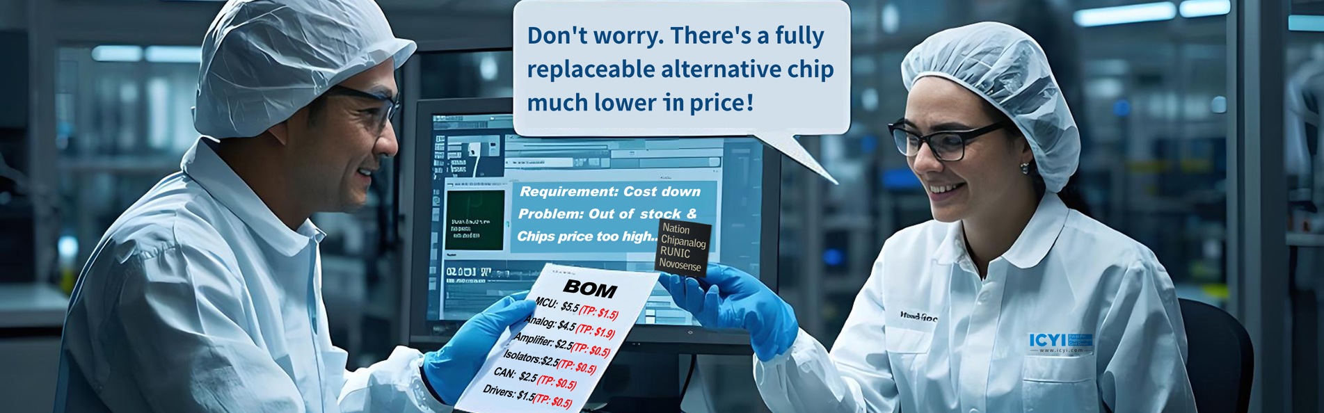
ST's SiC wafers and STM32 MCUs both adopt a dual supply chain strategy.
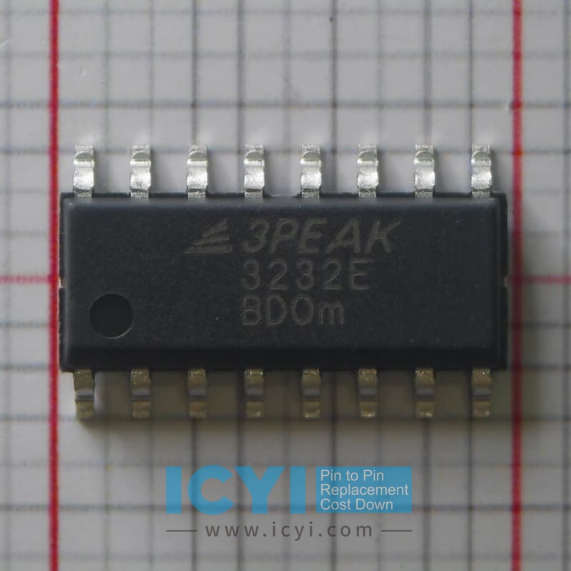
For SiC wafers, ST is laying out production capacity through joint ventures with local enterprises. ST and Sanan Optoelectronics have jointly established Anyifa Semiconductor in Chongqing, China. The joint venture factory plans to have an annual production capacity of 480000 8-inch silicon carbide wafers, mainly producing automotive grade electronic control chips. The joint venture factory adopts ST's SiC patented manufacturing process technology and selects locally produced SiC substrates in China. The packaging and testing of SiC devices are completed by STMicroelectronics Shenzhen Saiyifa, forming a complete localized 8-inch SiC supply chain in China.
For STM32 MCU, ST has chosen to cooperate with local wafer foundries. In November 2024, ST announced that it had commissioned Huahong to manufacture STM32 MCUs and other products with 40nm nodes in China to achieve localization of STM32. On this basis, ST's STM32 MCU can provide fully localized supply chain support for global OEM manufacturers operating in China, as well as supply chain options for Chinese OEM manufacturers operating internationally.
For gallium nitride (GaN) business. ST announced in March 2025 that it had signed a GaN technology development and manufacturing agreement with 8-inch silicon-based GaN manufacturer Innolux to collaborate on a joint development plan for GaN power technology. Based on a flexible supply chain layout, both parties will expand their respective GaN product portfolios and market supply capabilities, effectively enhancing supply chain resilience.
·NXP: Establishing a joint venture wafer fab in Singapore to expand its supply chain in China
NXP is also actively promoting the strategy of "in China, for China". On the one hand, NXP has established a joint venture, VSMC, with world leading companies in Singapore, a tariff friendly region of China; On the other hand, NXP announced in December 2024 that it plans to build a new supply chain in China and bring front-end manufacturing to China's domestic market.
The total investment of the VSMC project is approximately 7.8 billion US dollars (60% owned by World Advanced and 40% owned by NXP). VSMC's first 12 inch wafer fab uses 130nm to 40nm technology to produce mixed signal, power management, and analog products, supporting the needs of end markets such as automotive, industrial, consumer electronics, and mobile devices.
Last December, Andy Micallef, Executive Vice President of NXP, announced that the company was seeking to expand its supply chain in China to provide services to enterprises that require domestic supply chains in China. NXP stated at the time that it would relocate some of its chip front-end manufacturing to China and was exploring the possibility of establishing cooperation with local wafer foundries.
·Infineon: localizing production of commodity level products in China
At the end of last year, Infineon CEO Jochen Hanebeck stated that the company is localizing the production of commodity grade products in China, with the aim of strengthening close ties with customers in the Chinese market. On June 11, 2025, Infineon officially released its localization strategy of "in China, for China".
In terms of localized production, Infineon's automotive business has already completed localized mass production of multiple products. The company plans to cover the localization of major products by 2027, including microcontrollers, high and low voltage power devices, analog mixed signals, sensors, and storage devices. In order to better serve the Chinese automotive market and meet the increasing demand for MCUs from Chinese customers, the next generation 28nm TC4x product will be produced locally in China for both front-end and back-end production.
·US semiconductor IDM is also flexibly responding to tariff challenges
During the earnings conference call for the first quarter of 2025, Haviv Ilian, CEO of Texas Instruments, stated that the world is currently in a highly uncertain period, with tariffs and geopolitical factors disrupting the global supply chain and causing unpredictable economic conditions; China is not only an important terminal market, but also a key node in the global supply chain.
He also emphasized that the company has established a highly flexible supply chain system that can optimize production paths and reduce the impact of tariffs on costs. At present, TI adopts the "dual design" of its internal manufacturing process. For example, part of its embedded processors are produced by Taiwan, China's OEM factory, and the other part is produced by Lee Hai's factory in the United States. In the case of high tariffs between China and the United States, the products delivered by TI to Chinese customers are produced by Taiwan, China OEM. Global layout, process technology, and production capacity distribution of semiconductor IDM
The article "Global Layout and Capacity Inventory of Semiconductor Wafers (Part 1)" introduces Foundry's global layout and capacity distribution, with a focus on the global layout and distribution of semiconductor IDMs. The previous article introduced Samsung's situation, so this article will not elaborate further.
·Intel
1.1: Distribution of Intel's global manufacturing bases Image source: Intel official website
Intel proposed the "IDM 2.0" strategy in 2021, investing billions of dollars to lay out wafer fabs, attempting to regain the voice of chip manufacturing through a three pronged approach of "self construction+foundry+cooperation". In June 2023, Intel announced at an investor webinar that it had combined its Technology Development (TD), Contract Manufacturing, and IFS departments and required the department to be responsible for its own profits and losses. According to the plan, Intel's foundry business unit (IFS) will achieve breakeven by the end of 2030.
1.2: Intel's global wafer fab layout and process technology. As of late June 2025, Intel operates over 10 wafer fabs in 7 cities worldwide, mainly located in Arizona, Oregon, New Mexico, Ohio in the United States (awaiting mass production), Lexlip in Ireland, Jerusalem in Israel, and Saxony Anhalt in Germany (awaiting mass production); We operate testing plants in six cities worldwide, including Penang and Kulin in Malaysia, Chengdu in China, San Jose in Costa Rica, Ho Chi Minh City in Vietnam, New Mexico in the United States, and Wroc ł aw in Poland (awaiting mass production). ·Texas Instruments
2.1: Layout of Texas Instruments' global wafer fabs and packaging and testing facilities. Source: In recent years, Texas Instruments (TI) has continued to increase its investment in 12 inch (300mm) processes from 45nm to 130nm. The company has invested in the construction of seven new 12 inch (300mm) wafer fabs, which will bring improvements in scale, efficiency, and quality.
TI is building a new 12 inch semiconductor wafer manufacturing plant (SM1, SM2, SM3, SM4) in Sherman, Texas, with a total investment of $30 billion. After completion, the plant will produce millions of analog and embedded processing chips per day. Among them, SM1 will be put into operation as early as 2025.
2.2: Texas Instruments Global Wafer Plant Layout and Process Technology
In addition to wafer fabs, TI also owns and operates assembly and testing facilities worldwide, achieving regional diversification and controlling the supply chain on this basis. Currently, TI is investing in enhancing its assembly and testing capabilities, and improving the availability of manufacturing processes in multiple locations. TI has closed survey bases in Aguascalientes in Mexico, Kuala Lumpur and Malacca in Malaysia, New Taipei City in Taiwan, China, Baguio City in the Philippines, Clark Free Port District and other cities. It is expected that by 2030, over 95% of the company's wafer manufacturing, assembly, and testing operations will be transferred internally.
·SK Hynix
3.1: SK Hynix has production and manufacturing bases in four cities around the world. Image source: SK Hynix official website
SK Hynix was formerly known as Modern Electronics Industry Co., Ltd., established in 1983. After being acquired by SK Group in 2012, it was officially renamed SK Hynix Co., Ltd. SK Hynix is committed to producing semiconductor products primarily consisting of DRAM, NAND Flash, and CIS non memory. Currently, the company has four production bases in Lichuan and Cheongju, South Korea, Wuxi and Chongqing (closed testing factory), China, and sales, research and development bases in 16 countries and regions worldwide.
3.2: SK Hynix Global Wafer Plant Layout and Capacity
In recent years, SK Hynix has increased its business profits by building new production lines, renovating production lines, and relocating factories.
In terms of new production lines, SK Hynix plans to build four 12 inch wafer fabs in Longin City, Gyeonggi Province, South Korea, forming the Longin Semiconductor Cluster (Phase 1/2/3/4). Phase 1 is scheduled to be completed in May 2027 and will also build a "mini wafer fab" equipped with 300mm wafer processing equipment, providing a research environment for Korean component, material, and equipment suppliers to develop, showcase, and evaluate new technologies.
In terms of production line renovation, by the end of February 2025, SK Hynix will complete the renovation of its M10F factory in Licheon City, Gyeonggi Province, South Korea, and transform it into a production base for packaging HBM. The M10F factory adds HBM packaging capacity for 10000 wafers per month, increasing the total production capacity from 120000 wafers to 130000 wafers. It is expected that by the end of 2025, with the commissioning of the M15X factory in Qingzhou City, the total production capacity will reach 160000 to 170000 wafers.
In terms of factory relocation, SK Hynix System IC (formerly known as SK Hynix Foundry Business Unit) will relocate its M8 factory located in Cheongju, South Korea to Wuxi, China and rename it for registration before May 2022. M8 factory has a monthly production capacity of 100000 8-inch wafers, producing DDI, PMIC, and CIS. Original M8 factory produces DDI for LG LCD screens, PMIC for Silicon Mitus, and CIS for SK Hynix.
SK Hynix also has a packaging and testing factory in Chongqing, China - Aisikai Hynix Semiconductor (Chongqing) Co., Ltd., which mainly produces Nand Flash, a flash memory product suitable for mobile terminals. The product is mainly used in mobile terminal devices such as smartphones, tablets, USB, etc. ·Meiguang
4.1: Micron's global wafer fab layout and production capacity. Micron's headquarters is located in Boise, Idaho, and its wafer fabs are spread across Boise, Idaho in the United States, Taichung in Taiwan, Hiroshima in Japan, and Singapore. According to the news released by Micron in mid June 2025, the company plans to invest $200 billion to support semiconductor manufacturing and research and development in the United States, introducing HBM manufacturing to the domestic market.
It is reported that Micron will start building the Boise wafer fab in October 2023 and begin producing DRAM in 2027. Now, the company plans to build a second wafer fab in Boise, expected to be completed and put into operation before the first wafer fab in New York State, and to create synergies with existing production lines. After the completion of the two factories, the HBM packaging project will be launched.
Over the past few decades, Micron has also expanded its business through continuous mergers and acquisitions. In 2010, the company acquired Numonyx, a flash chip manufacturer, for $1.27 billion; In 2013, Micron acquired Elpida Memory and expanded its memory business; In 2016, Micron also acquired PC memory manufacturers Rexchip and Innotera Memories; In 2024, Micron acquired AU's wafer fabs in Taichung and Tainan to support its DRAM production business in Taichung and Taoyuan factories.
The Hiroshima plant in Japan is a facility that was acquired after the merger with Erbida. By 2025, the Hiroshima plant will produce 1 gamma DRAM, and in addition, it will also produce HBM. According to the plan, Micron will also build a new DRAM chip manufacturing plant in Hiroshima and introduce EUV equipment, with advanced DRAM being mass-produced as early as the end of 2027; Micron Taichung Plant 4 was acquired from AU Optronics, and together with A3 Plant, it forms Micron's vertically integrated DRAM manufacturing base in Taiwan. Based on this, Micron Taichung Plant will increase its monthly wafer production to 60000 pieces by the end of 2025. ·STMicroelectronics
4.2: ST's front-end/back-end factory layout supports global enterprises' multi wafer procurement strategy (information updated as of March 2025) Image source: ST STMicroelectronics' wafer manufacturing plants are mainly concentrated in Europe and Asia, specifically distributed in Norrkoping, Sweden, Crolles, Rousset, Tours in France, Agrate and Catania in Italy, Chongqing, Singapore and other regions in China. In addition, ST also has semiconductor sealing and testing plants in cities such as Rennes in France, Marcianise in Italy, Bouskoura in Morocco, Kirkop in Malta, Shenzhen in China, Muar in Malaysia, and Calamba in the Philippines.
5.1: STMicroelectronics' global wafer fab layout and production capacity. Based on the layout of the front/back processes mentioned above, ST can support global enterprises' multi wafer procurement strategies. For customers who are very concerned about the origin of wafers, ST will prioritize providing wafers from the required origin for these customers; For some customers who are not sensitive to their origin, ST will coordinate the entire global supply chain.
Now, ST is actively promoting the upgrade plan of its SiC wafer fab, with the core goal of gradually upgrading the original 6-inch production line to an 8-inch production line starting from Q3 2025. For example, its Catania factory in Italy will transition from 6-inch to 8-inch production processes in Q3 2025; Subsequently, the Singapore factory will also initiate an upgrade to 8-inch SiC wafer production within 2025. This move aims to consolidate its leading position in the rapidly growing high-performance power semiconductor market by improving production efficiency and reducing costs, and to coordinate with its dual supply chain system construction strategy. ·NXP
NXP currently has 8 wafer fabs (including 4 planned to close 8-inch fabs). Due to the high cost and outdated technology of 8-inch fabs (all of which are mature processes above 100nm), the company is gradually phasing out 8-inch fabs and shifting towards 12 inch fabs. Among the four 8-inch wafer fabs that NXP will close, one is located in Nijmegen, the Netherlands, and three are located in the United States. After the closure, production capacity will be relocated to the 12 inch production lines of the VSMC and ESMC joint ventures.
5.2: NXP's global wafer fab layout (excluding the planned closure of 4 8-inch wafer fabs) In the future, NXP may reduce to 5 core fabs. In addition, NXP has invested $7.8 billion in its joint venture plant in Singapore (VSMC, planned for mass production in 2027), focusing on 130nm-40nm mixed signal and power management chips, with a monthly production capacity of 55000 wafers by 2029; NXP also has a joint venture wafer fab ESMC in Germany, but it only holds a 10% stake and is operated by TSMC (which holds a 70% stake). The total investment of the fab exceeds 10 billion euros, with a planned monthly production capacity of 40000 12 inch wafers. Construction will begin in the second half of 2024 and production will begin at the end of 2027. ·Infineon
6: Distribution of Infineon's 15 factories (including front-end and back-end factories, data as of September 30, 2024) Image source: Infineon has a total of 15 factories worldwide (including front-end and back-end factories) as of September 30, 2024. Among them, the United States has gathered several production bases of Infineon, with wafer fabs located in Austin, Texas and Mesa, Arizona. At the end of February 2025, the company announced the sale of its 8-inch wafer fab Fab25 located in Austin, Texas, to SkyWater. It is reported that Fab25 focuses on producing 130nm to 65nm basic chips that are crucial for industrial, automotive, and defense applications.
7: Infineon's global wafer fab layout (incomplete statistics). Infineon also has front-end wafer fabs in Kulin Malaysia, Regensburg and Dresden in Germany, and Filach in Austria. Among them, the K3 wafer fab in Kulin, Malaysia is an 8-inch SiC wafer fab. Phase 1 has been put into operation since August 2024, with initial production capacity focused on SiC power semiconductors. It is expected that after Phase 2 is put into operation, the total production capacity will increase to the world's largest scale, covering the production of gallium nitride epitaxy; The Smart Power Fab in Dresden, Germany is the world's first semiconductor factory to comply with Industry 4.0 standards, covering wafer processing, testing, and separation processes; It is planned to start production in 2026 and is expected to reach full capacity production by 2031.
·Ansenmei
Figure 6: Anson's manufacturing factories are scattered in 9 countries around the world. Image source: Anson has 19 production factories (including front-end and back-end processes) in 9 countries, located in the United States, Canada, China, Czech Republic, Japan, Malaysia, Philippines, South Korea, and Vietnam.
Anson Semiconductor was originally part of Motorola's semiconductor division, spun off from Motorola in 1989, and went public on NASDAQ in 2000. The 6-inch wafer fab in Roznov, Czech Republic, the 6-inch wafer fab/packaging and testing plant in Seremban, Negeri Sembilan, Malaysia, and the packaging and testing plant in Kamona, Krabi Province, Philippines, which are still in operation, are all factories that were spun off from Motorola at that time.
8: Anson's global manufacturing base layout (including wafer fabs and packaging and testing facilities). In addition, most of the wafer fabs/packaging and testing facilities currently operated by Anson are acquired through mergers and acquisitions. Including its 12 inch wafer fab located in East Fishkill, New York, which was acquired in 2019 through the purchase of the Grosvenor Fab10 wafer fab, and its 8-inch wafer fab located in South Par, Iowa, which was acquired in 2014 through the purchase of Aptina Imaging. In addition, its 8-inch wafer fabs located in Gresham, Oregon, Mentintop, Pennsylvania, Shenzhen, Guangdong, China, and Wakamatsu, Japan, as well as its 8-inch/6-inch wafer fabs in Bucheon, Gyeonggi Province, South Korea, and its packaging and testing plants in Tongna, Vietnam, Tarak, Philippines, and Burlington, Ontario, Canada, all came from mergers and acquisitions. ·ADI
Figure 7: ADI Global Manufacturing Base and Supply Chain Network Image Source: ADI's product supply chain is mainly completed through the collaboration of "independent wafer fabs+external foundries". The company has deployed 10 independent factories (including front-end and back-end factories) and 50 supply chain factories worldwide, covering 15 countries or regions. The front-end wafer fabs within ADI lead mature processes (Beaverton, Oregon/Limerick, Ireland, USA), and their advanced process technologies are mainly provided by their foundry partners.
9: ADI's internal manufacturing base layout (including wafer fabs and packaging and testing plants) Overall, ADI's internal factories contribute about 50% of wafer production capacity, 80% of testing capacity, and 20% of packaging capacity. Currently, ADI is expanding its wafer fab capacity through internal investment. It is expected that by the end of 2025, the production capacity of wafer fabs located in the United States and Europe will double - the Beaverton factory in Oregon is renovating an 8-inch wafer fab, increasing its cleanroom area by 25000 square feet and doubling its production capacity; The production area of the Limerick factory in Ireland will be expanded by 15000 square feet, with a threefold increase in production capacity; The Camus factory in Washington state is also expanding its production capacity.
Most of the testing work for ADI products is conducted in factories in the Philippines, Malaysia, and Thailand, and the assembly business is outsourced to trusted partners. ADI is expanding its testing facilities in Malaysia and Thailand, and has also expanded its campus in the Philippines. In addition, ADI is cross validating testing processes with external partners to ensure that dual procurement can be conducted when needed. ·Microchip Technology
Microchip's hybrid supply chain strategy combines US wafer manufacturing plants with global assembly facilities, fully utilizing internal and external foundries and OSAT manufacturers. With the support of strategic partnerships, this manufacturing ecosystem can optimize the production of high-value markets while balancing cost-effectiveness and reliability.
In May 2025, Microchip closed its Fab2 wafer fab in Tempe, Arizona, which has a monthly production capacity of 20000 8-inch wafers (1 μ m-250nm process). Its technology and products will be transferred to Fab4 and Fab5 factories. At the same time, Fab4 and Fab5 factories have laid off employees, and the production capacity of the two wafer fabs has been reduced to below short-term demand levels. After the excess inventory is digested, it will gradually return to demand matching production capacity. Fab4 will still maintain a two-week preparation time for resuming production after the layoffs.
10: Global wafer fab layout and current situation of Microchip Technology. In addition, the company's packaging and testing bases are distributed in the United States (Beverly, Massachusetts; Lawrence and Lowell, Massachusetts; Holly Springs, Pennsylvania; San Jose and Garden Grove, California; Simsbury, Connecticut), France, the United Kingdom, Ireland, Germany, Thailand, the Philippines, and other places.