Blog
Striving to be the "game-changer" in China's analog chip industry, Novosense is heading towards the global market
The chip industry continues to develop, and China's path of independent research and development is thriving. Novosense, as a core enterprise in domestic analog chips, is leading the way. Not only has it continuously increased its market share in China, but it has also become a key player in the global supply chain, and together with a group of outstanding Chinese chip companies, it is changing the industry landscape.
How can Chinese chip companies grow from scratch to 1, and then from 1 to 10,000? Recently, Yao Di, Vice President of Novosense, stated in a recent external exchange that Novosense's "Rooted in China, Expanding to the World" relies on systematic capabilities. Currently, the company has already deployed some overseas production capacity, providing leading products to the market based on reliability and efficiency.
Accuracy, reliability, and response efficiency constitute the "moat" of Novosense
The competition in the global analog chip market is essentially a dual contest of "performance + trust". Yao Di believes that Novosense has been able to break through from hundreds of domestic enterprises and become a partner of leading enterprises in the global automotive, industrial, and other fields, primarily because it has built a solid "moat" in three dimensions: precision, reliability, and response efficiency.
Accuracy is the "core soul" of analog chips, directly determining the "sensory ability" of electronic systems.
Yao Di cited the "gain with speed" function of cars as an example. The analog chip needs to first sense physical signals such as vehicle speed and external noise, transmit them to the central control system, and then send instructions to "increase/decrease volume" to the speaker. In this process, the accuracy and sensitivity of signal conversion directly affect the functional experience. "Just like a hand touching a lit candle will immediately withdraw, if the reaction is 1 second slow, the skin tissue may be burned," the analog chip has extremely high requirements for signal response speed and sensitivity.
Novosense has deeply invested in high-precision technology, developing chips capable of accurately converting physical signals into electrical signals. Whether it's voltage acquisition for automotive battery management systems or temperature detection for industrial equipment, these chips can meet customers' stringent accuracy requirements. This is one of the key reasons why many customers choose Novosense for their smart driving system collaborations.
Reliability is the "bottom line" for analog chips, especially in long-life scenarios such as automotive and industrial applications, where no compromise is acceptable.
Yao Di emphasized that while an automobile may only have 1-2 "brains" (main chips), the number of analog chips can range from hundreds to thousands. "If even one of these analog chips malfunctions, the entire system could potentially break down." Moreover, considering that automobiles typically have a lifespan of 10-20 years, these analog chips must also withstand harsh environments such as high temperatures and high-frequency vibrations in the engine compartment.
To this end, Novosense has invested significantly more resources than the industry average to establish a reliability control system: the proportion of quality team members has been maintained at 8%-10% for a long time; in the production process, strategic cooperation has been established with leading global wafer fabs and packaging and testing factories to ensure quality from the source; at the same time, a large number of quality resident teams and engineering resident teams have been stationed in foundries for long-term monitoring of the quality of every production process, including encapsulation and pin extraction.
Its automotive-grade chips have passed rigorous testing and demonstrated excellent long-term stability, which is why top-tier wafer fabs choose to deeply collaborate with Novosense. Only a reliable design solution can fully leverage the value of advanced manufacturing processes.
03 Response efficiency is a "differentiating advantage" for Novosense and even Chinese chip companies in global competition. Chinese companies possess a "speed" that overseas giants lack.
Yao Di mentioned that Novosense can quickly customize and develop products according to customers' personalized needs. This agility is particularly important in the rapid iteration of the automotive industry. Faced with urgent supply demands, Novosense can efficiently leverage supply chain resources such as wafer fabs and packaging factories, and achieve rapid response through a mature collaborative mechanism. This demonstrates the flexibility of delivery in automotive chip applications and lays the foundation for further deepening cooperation.
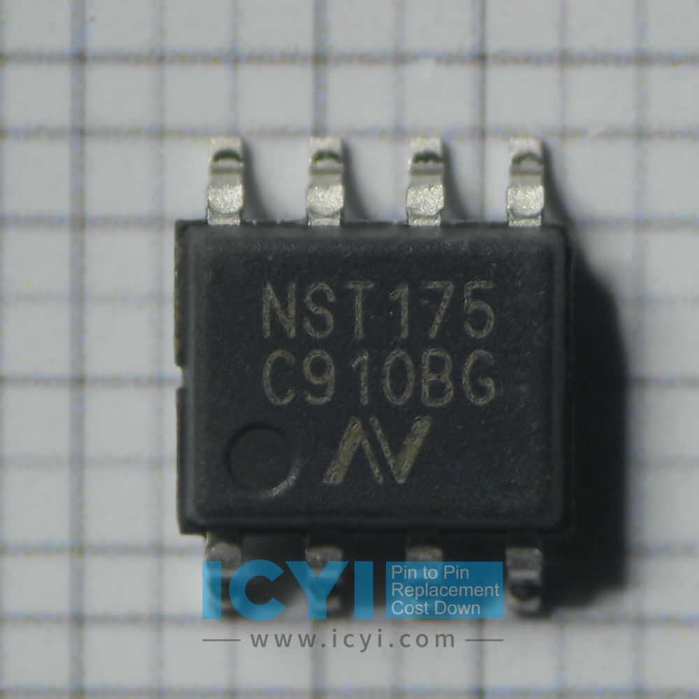
The analog chip is currently undergoing reliability testing
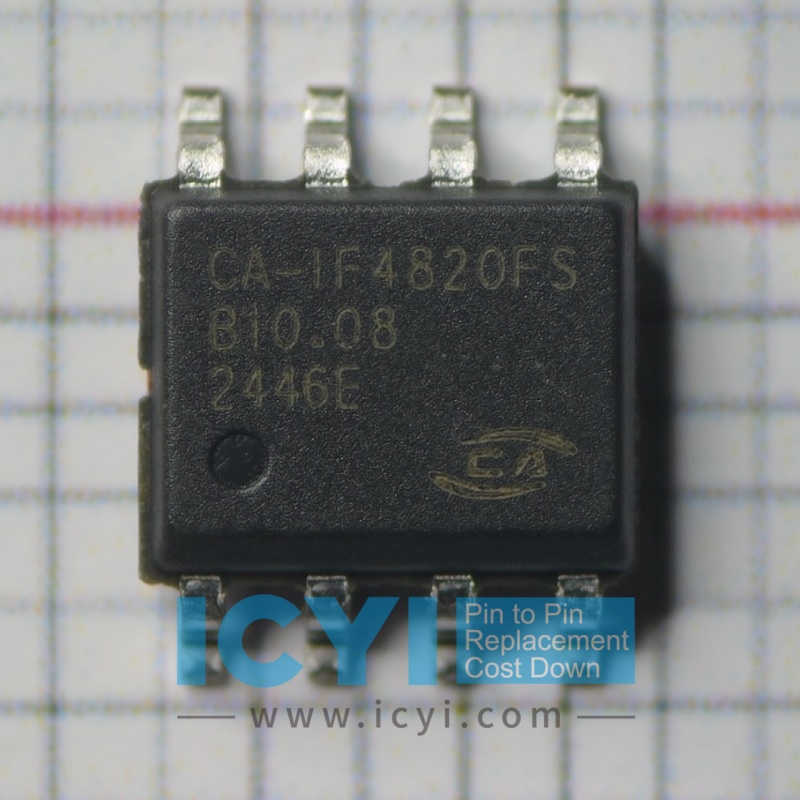
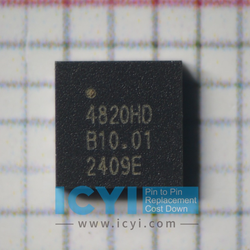
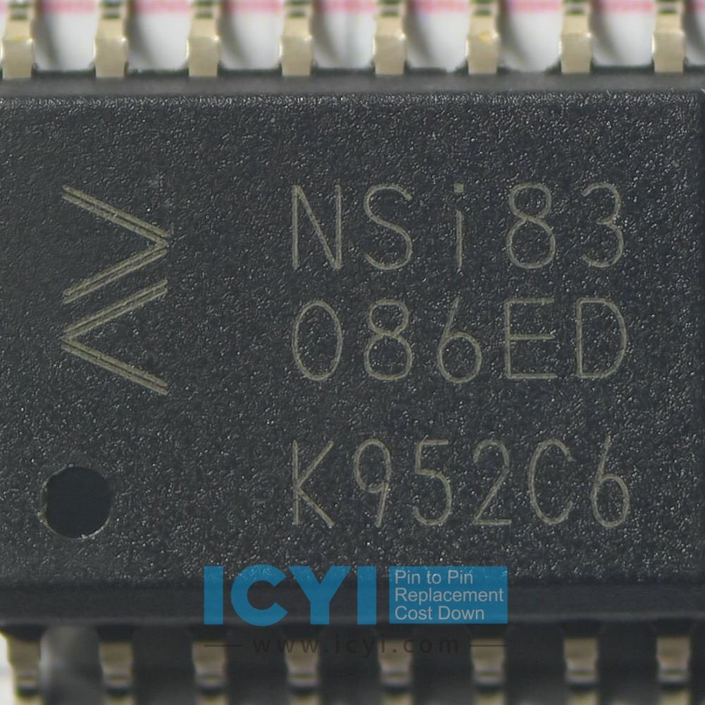
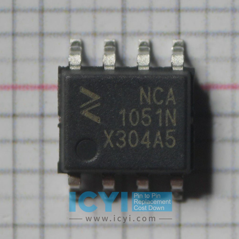
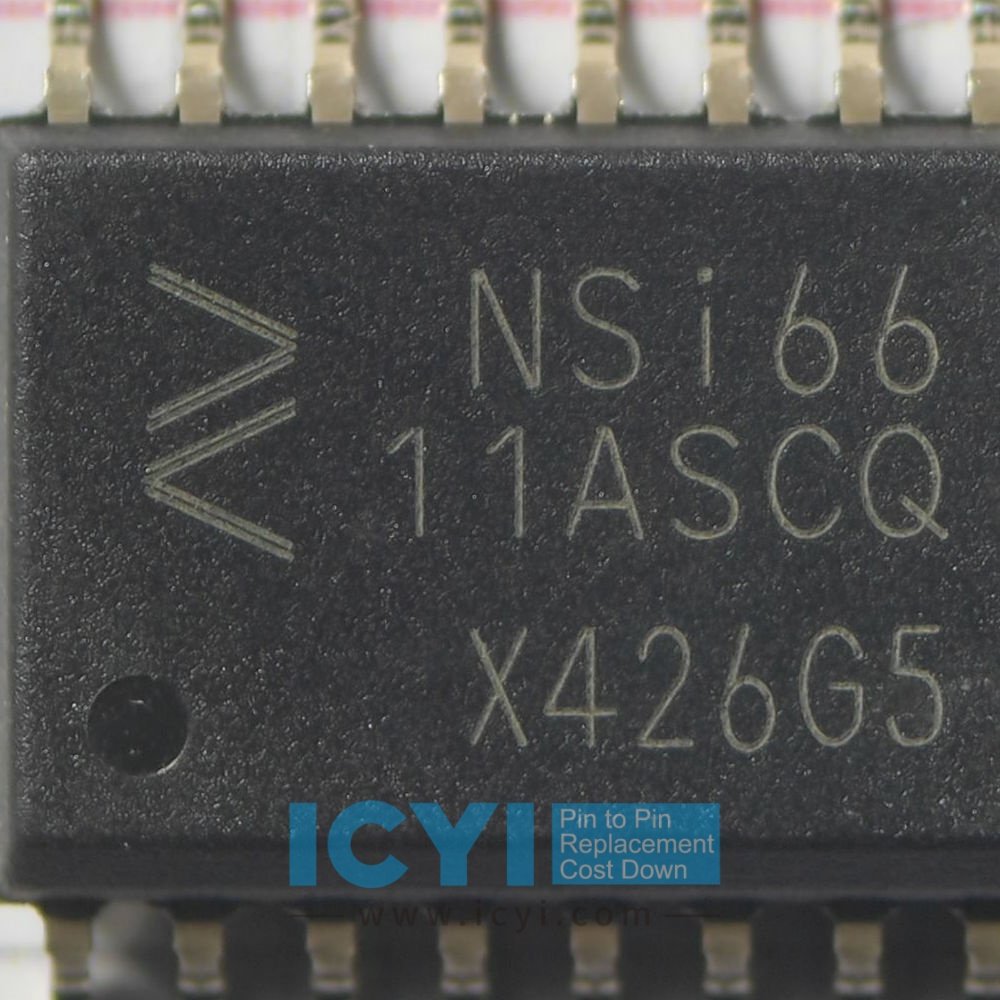
Novosense hot sale part numbers in the global market:
NSI8210N0-DSPR
NSI8210N1-Q1SPR
NSi8120N0/NSI8220N0-DSPR
NSi8120N1
NSI8220N1-DSPR
NSi8141W1
NSI8241W1-DSWR
NSi8141S0
NSi8141S1
NSI8260W0-DSWR
NSi8261S1-DSSR
NSi8262W0-DSWR
NSi8262W1-DSWR
NSi8100W
NSI1050-DDBR (DUB8)
NSI1050-DSWR (SOW16)
NCA1042-DSPR
NCA1051N-DSPR
NSD1025-DSPR
NSD1624-DSPR
NSi6801TC-DDBR (DUB8)
NSI6611ASC-Q1SWR
NSI1311-DSWVR
NSI1300D05-DSWVR
NSi1200-DSWVR
NSI1306M25-DSWR