Entering the "post AI" era, HBM is no longer just a standard component for high-performance AI chips such as GPUs and TPUs, but has evolved into a strategic high ground for fierce competition among semiconductor giants.
Whether it's Samsung, SK Hynix, or Micron, these leading companies in the storage field all unanimously see HBM as a key engine for future revenue growth. They seem to have reached a consensus that in order to dominate the storage market, they must first master the core technology of HBM.
So, in this competition without gunpowder, what technologies are worth paying attention to? Let's delve into the analysis together.
Is customization the only way out?
Customization may be one of the ultimate destinations of HBM.
In fact, more than two years ago, when HBM was first emerging, Hynix and Samsung discussed the trend of customization. With cloud giants customizing their own AI chips, the demand for HBM has only increased and not decreased, making customization one of the inevitable needs.
In August last year, SK Hynix Vice President Yoo Sung soo stated, "All M7 (Magnificent 7) refers to the seven major tech stocks in the S&P 500 index: Apple, Microsoft, Google Alphabet, Amazon, Nvidia, Meta, and Tesla. )Companies have come to us requesting customized HBM (High Bandwidth Memory). ”
In June of this year, South Korean media reported that SK Hynix had simultaneously targeted companies such as Nvidia, Microsoft (MS), Broadcom, which are expected to become "heavyweight customers" in the customized HBM market. It has recently reached agreements with Nvidia, Microsoft, and Broadcom to supply customized HBM and has begun design work based on the needs of each company.
It is reported that SK Hynix prioritizes the supply plan of its largest customer NVIDIA and determines the list of other customers. Industry insiders have stated that "considering SK Hynix's production capacity and the launch schedule of AI services from major technology companies, it is not possible to meet the needs of all M7 customers at once," but also pointed out that "considering the changes in the HBM market situation, there may be several new customers added in the future.
SK Hynix also announced in April this year that it will shift towards customization starting from the seventh generation HBM (HBM4E) and has partnered with TSMC. We plan to adopt TSMC's advanced logic technology on the HBM4 basic die, and it is expected that the first batch of customized HBM products will be launched in the second half of next year,
It is worth mentioning that due to SK Hynix's successful acquisition of multiple heavyweight clients, its likelihood of maintaining its dominant position in the next-generation customized HBM market has greatly increased. According to TrendForce data, SK Hynix currently holds a market share of approximately 50% in the HBM market, far surpassing Samsung Electronics (30%) and Micron (20%). If we only look at the latest HBM3E product, SK Hynix's market share is as high as 70%.
On the other hand, Samsung Electronics has also been exposed to be in discussions with multiple customers regarding the supply of customized HBM. Given its recent success in supplying HBM3E to AMD, the world's second-largest AI chip manufacturer, the industry expects it to soon acquire customers for HBM4 and custom HBM as well. It is reported that Samsung is currently in specific negotiations with customers such as Broadcom and AMD regarding the HBM4 product.
Compared to the two Korean manufacturers, Micron, located far away in the United States, appears much slower. In June of this year, Raj Narasimhan, Senior Vice President and General Manager of Micron Cloud's Memory Business Unit, stated that the production plan for HBM4 will be closely integrated with the readiness of customers' next-generation AI platforms to ensure seamless integration and timely expansion of production to meet market demand.
It stated that in addition to providing the latest HBM4 to mainstream customers, customers are also seeking customized versions, and the development of the next generation HBM4E is also underway. Collaborating with specific clients to develop customized HBM solutions will further enhance the value of memory products.
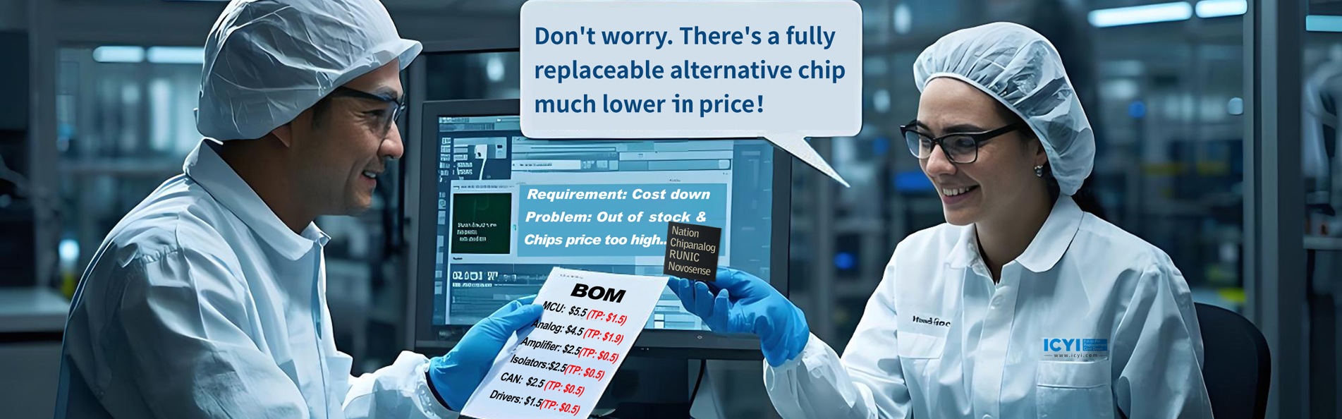
At this point, many people may want to ask, what are the benefits of customizing HBM, and why are DRAM manufacturers and cloud giants flocking to it?
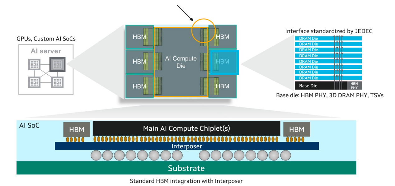
Firstly, it needs to be clarified that the key to customizing HBM (cHBM) lies in integrating the functionality of the base die into the logic die designed by the SoC team. This includes controlling I/O interfaces, managing DRAM stacks, and carrying direct access (DA) ports for diagnosis and maintenance.
This integration process requires close collaboration with DRAM manufacturers, but it gives SoC designers greater flexibility and stronger control over access to the HBM core chip stack. Designers can integrate memory and processor chips more tightly and optimize between power consumption, performance, and area (PPA) based on specific applications.
SoC designers can freely configure and instantiated their own HBM memory controllers, and directly interact with the HBM DRAM stack through DFI2STSV bridging. Logic chips can also integrate enhanced features such as programmable high-quality built-in self-test (BIST) controllers, chip to chip adapters (D2D adapters), and high-speed interfaces (such as the universal chip to chip interconnect standard UCIe), enabling communication with processor chips in a complete 3D stack. Due to the fact that the chip is manufactured using logic processes rather than DRAM processes, existing designs can be reused.
One important advantage of customizing HBM is to significantly reduce the delay introduced by the intermediary in the data path, thereby reducing related power consumption and performance losses. It effectively shortens the distance between memory and processor chips by reusing existing high-speed bare chip interconnects (such as UCIe). This flexibility can be applied to various scenarios, such as cloud service providers using edge AI applications with extremely high cost and power requirements, as well as systems pursuing maximum capacity and throughput for complex AI/machine learning computing scenarios.
However, customized HBM currently faces some challenges, as its entire concept is still emerging and the technology is in the early stages of development. Like all innovations, the road ahead is inevitably accompanied by challenges. Integrating basic chip functions into logic chips means that end users need to consider the entire lifecycle from the perspective of chip lifecycle management (SLM) - from design, trial production, mass production, to on-site applications. For example, after wafer level HBM chip stacking, the responsibility for screening DRAM cell defects will fall on end users. This raises some questions, such as how should users handle specific DRAM algorithms recommended by suppliers? And can users conduct comprehensive on-site testing and diagnosis of HBM during planned downtime?
At present, to successfully deploy customized HBM, a complete ecosystem is needed, which brings together IP providers, DRAM manufacturers, SoC designers, and ATE (Automated Test Equipment) companies. For example, due to the large number and high density of interconnections, traditional ATE can no longer be used for customized HBM testing.
In summary, customized HBM has become a major trend, and regardless of whether manufacturers like it or not, it will occupy a significant position in the HBM4 standard.
The technical challenge of mixed bonding that cannot be bypassed?
In addition to customization, hybrid bonding is also one of the important development directions for HBM in the future.
At present, with the continuous increase of stacking layers, traditional welding techniques are facing significant challenges. The flux currently used can remove metal surface oxides and promote solder flow, but its residues can cause problems such as increased stack gaps and thermal stress concentration, especially in precision packaging fields such as high bandwidth memory (HBM), where this contradiction is more prominent.
And even Samsung, SK Hynix, and Micron are considering using hybrid bonding technology in the next generation HBM.
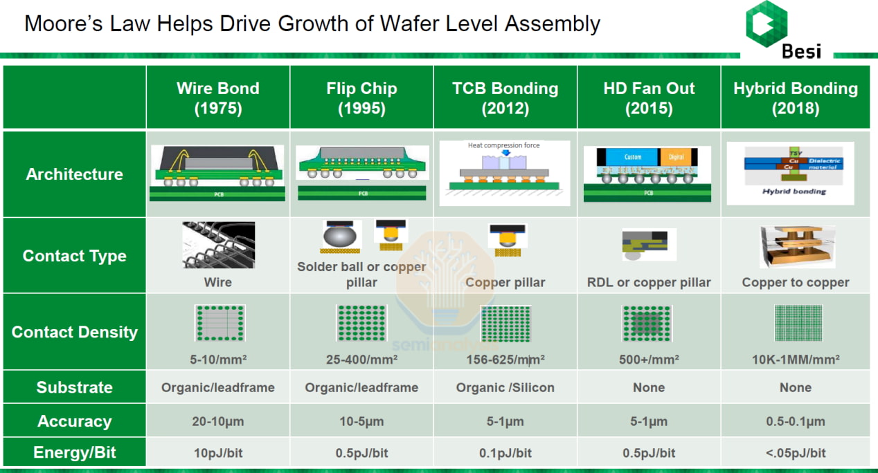
Let's first understand the current bonding technology of HBM chips. In traditional flip chip bonding, the chip is "flipped" so that its solder bumps (also known as C4 bumps) align with the bonding pads on the semiconductor substrate. The entire component is placed in a reflow oven and uniformly heated to around 200 º C-250 º C according to the solder material. The solder bump melts, forming electrical interconnection between the joint and the substrate.
With the increase of interconnect density and the reduction of spacing to below 50 µ m, the flip chip process faces some challenges. Due to the entire chip package being placed in an oven, the chip and substrate will expand at different rates (i.e., different coefficients of thermal expansion, CTE) due to heat, resulting in deformation and interconnect failure. Then, the molten solder will spread beyond its designated area.
This phenomenon is called solder bridging, which can cause unnecessary electrical connections between adjacent pads and may result in short circuits, leading to chip defects. This is where the TCB (Thermal Compression Bonding) process comes into play, as it can solve the problem of flip chip technology when the spacing is reduced below a certain point.
The advantage of TCB is that heat is locally applied to the interconnect points through the heating tool head, rather than uniformly applied in the reflow soldering furnace (flip chip). This can reduce the heat transfer to the substrate, thereby reducing thermal stress and CTE challenges, and achieving stronger interconnections. Apply pressure to the chip to improve bonding quality and achieve better interconnection. The typical process temperature range is between 150 º C-300 º C, and the pressure level is between 10-200MPa.
TCB allows for a higher contact density than flip chip, reaching up to 10000 contact points per square millimeter in some cases, but the main drawback of higher precision is lower throughput. Although the flip chip machine can achieve a throughput of over 10000 chips per hour, the throughput of TCB is in the range of 1000-3000 chips.
The standard TCB process also requires the use of soldering flux. During the heating process, copper may oxidize and cause interconnect failures, and flux is a coating used to remove copper oxides. But when the interconnect spacing is reduced to 10 µ m or more, the flux becomes more difficult to remove and leaves sticky residue, which can cause minor deformation of the interconnect, leading to corrosion and short circuits.
Fluxless bonding technology emerged as a result, but it can only further reduce the spacing size to 20 μ m, up to a maximum of 10 μ m, and can only be used as a transitional technology. When the I/O spacing is less than 10 μ m, hybrid bonding technology is required.
Hybrid bonding technology achieves DRAM chip stacking through copper to copper bonding, eliminating the need for traditional bump structures. This approach not only significantly reduces chip size but also doubles energy efficiency and overall performance.
According to industry insiders, as of May 7th, Samsung Electronics and SK Hynix are advancing the use of hybrid bonding technology for mass production of their next-generation HBM products. It is expected that Samsung will adopt this technology in the HBM4 (sixth generation HBM) as early as next year, while SK Hynix may be the first to introduce it in the seventh generation product HBM4E.
The current fifth generation HBM - HBM3E still uses hot press bonding technology to fix and stack chips through heating, pressure, and bump connections. Samsung mainly purchases TC equipment from its subsidiary SEMES and Japan's Shinkawa Electric (SHINKAWA), while SK Hynix relies on Hanmei Semiconductor and Hanhua Semiconductor. Micron, which provides HBM to Nvidia, also purchases equipment from South Korea, the United States, and Xinchuan.
With the initial opening of the hybrid bonding market, this technology is expected to trigger a major reshuffle in the semiconductor equipment field. Once successfully imported, hybrid bonding may become the mainstream process for future HBM stacking.
In order to seize the opportunity, an American application materials company has acquired a 9% stake in Besi, the only company in the world with advanced production capabilities for hybrid bonding equipment, and has taken the lead in introducing its hybrid bonding equipment into the system level semiconductor market, seizing the application opportunity.
At the same time, Hanmei Semiconductor and Hanhua Semiconductor are also accelerating the development of next-generation chip stacking equipment. These two Korean manufacturers are not only rapidly advancing the research and development of hybrid bonding equipment, but also actively developing solder bonding equipment to enhance market competitiveness.
If customized HBM is a struggle between DRAM manufacturers and cloud giants, then hybrid bonding is a game between DRAM manufacturers and bonding device manufacturers. With HBM officially entering the HBM4 era in the second half of this year, the attention to hybrid bonding may further increase.
What other new technologies are there?
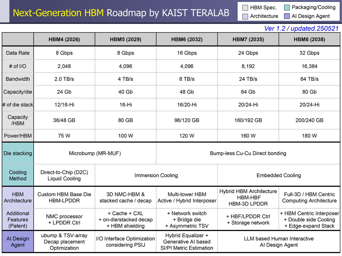
It is worth mentioning that in June of this year, the Korean Academy of Sciences and Technology (KAIST), a national research institution in South Korea, released a 371 page research paper systematically depicting the evolution path of HBM technology from HBM4 to HBM8. The content covers improvements in bandwidth, capacity, I/O interface width, thermal design, as well as packaging methods, 3D stacking structures, memory center architectures for embedded NAND storage, and even machine learning based power control methods.
It is worth emphasizing that this document is not a product roadmap released by a commercial company, but an academic prediction of the potential evolution of future HBM technology based on current industry trends and scientific research progress. However, it is also enough to give us a glimpse into the possible development direction of HBM in the future.
Let's first take a look at the technical features of each generation of products from HBM4 to HBM8:
HBM4: Pioneer of Customized Design. As the beginning of the new generation of HBM technology, HBM4's biggest innovation lies in customized basic die design. By integrating NMC (Near Memory Computing) processors and LPDDR controllers, HBM4 enables direct access to HBM and LPDDR without the need for CPU intervention. This design significantly reduces data transmission latency and improves overall system efficiency.
HBM4 supports multiple flexible data transfer modes, including direct read and write between GPU and HBM, data migration between HBM and LPDDR, and GPU indirect access to LPDDR through HBM. The introduction of dual command execution capability further enhances the efficiency of multitasking and provides strong support for complex AI workloads.
HBM5: Breakthrough in 3D Near Memory Computing HBM5 pushes 3D Near Memory Computing technology to new heights. By integrating NMC processor die and cache die, and using dedicated TSV interconnects and power networks, HBM5 achieves a highly energy-efficient computing architecture. The introduction of distributed power sources/grounding and thermal TSV arrays effectively reduces IR voltage drop and improves heat dissipation efficiency.
Of particular note is the introduction of AI design agent optimization technology in HBM5, which utilizes intelligent algorithms to optimize TSV layout and decoupling capacitor placement, significantly reducing power supply noise induced jitter (PSIJ). This innovation not only enhances system stability, but also lays the foundation for the intelligent design of subsequent products.
HBM6: Innovation in Multi Tower Architecture The biggest highlight of HBM6 is the introduction of the Quad Tower architecture. Four DRAM stacks share a basic die, achieving an astonishing bandwidth of 8 TB/s through 8096 I/O channels. This architecture design not only improves bandwidth performance, but also enhances cost-effectiveness through resource sharing.
The integration of L3 cache is another important innovation of HBM6. By reducing the need for direct access to HBM, L3 caching significantly improves the inference performance of LLM. Actual test data shows that the L3 cache embedding of HBM6 reduces HBM access by 73% and latency by 87.3%. The introduction of a crossover switch network enables HBM cluster interconnection, optimizing the high throughput and low latency LLM inference performance.
HBM7: Hybrid Storage Ecosystem HBM7 has built a complete hybrid storage ecosystem. By integrating high bandwidth flash memory (HBF), a HBM-HBF storage network is formed with a total capacity of 17.6 TB, which can meet the storage needs of large-scale AI inference. The combination with 3D stacked LPDDR further expands the storage hierarchy, achieving an interconnect bandwidth of 4096 GB/s on the glass intermediate layer.
The comprehensive application of embedded cooling structure is an important feature of HBM7. Efficient heat transfer from the chip to the cooling fluid has been achieved through thermal transmission lines and fluid TSV technology. The introduction of LLM assisted interactive reinforcement learning (IRL) technology makes decoupling capacitor placement and PSIJ optimization more intelligent and precise.
HBM8: In the era of full 3D integration, HBM8 represents the pinnacle of HBM technology, achieving true full 3D integration and HBM center computing. The double-sided intermediate layer design supports various 3D extension architectures such as GPU-HBM-HBM, GPU-HBM-HBF, and GPU-HBM-LPDDR, providing flexible configuration options for different application scenarios.
The fully 3D GPU-HBM integrated architecture is the core innovation of HBM8, with the GPU located at the top of the storage stack, which not only facilitates heat dissipation but also achieves seamless integration of storage and computing. The comprehensive application of AI design agents makes 3D layout and routing optimization more intelligent, considering the collaborative optimization of thermal signal integrity.
From the overall development trend, the evolution of HBM technology shows a significant leap in magnitude. In terms of bandwidth, there has been an astonishing 32 fold increase from HBM4's 2.0 TB/s to HBM8's 64 TB/s. This breakthrough is mainly achieved through two dimensions: first, a significant increase in the number of I/Os, from 2048 to 16384; The second is the steady increase in data rate, from 8 Gbps to 32 Gbps.
In terms of capacity expansion, the single module capacity has been increased from 48 GB for HBM4 to 240 GB for HBM8, achieved through an increase in stacking layers and single die capacity. At the same time, the power consumption gradually increased from 75W to 180W. Although the power consumption has increased, considering the significant improvement in performance, the overall energy efficiency ratio still shows significant improvement.
Key technological innovation path
Another significant feature of the evolution of HBM technology is the continuous breakthrough of 3D integration technology. Starting from HBM4, the technological roadmap gradually transitioned from traditional micro bump bonding to non bump Cu Cu direct bonding technology. This transformation not only significantly reduces contact resistance, but also greatly increases interconnect density, laying the foundation for subsequent high-density 3D stacking.
TSV (Through Silicon Via) technology, as the core of 3D integration, enables efficient electrical connections between vertically stacked bare chips. By shortening the interconnect length, TSV technology effectively reduces RC latency and power consumption, providing hardware support for high bandwidth data transmission. At the HBM8 stage, the introduction of coaxial TSV technology further enhances signal integrity and supports high-speed data transmission at 32 Gbps.
The development of intermediary technology is also remarkable. From a single silicon intermediate layer to a silicon glass hybrid intermediate layer, this innovation breaks through the size limitation of pure silicon intermediate layers while maintaining excellent signal integrity. The hybrid intermediate layer technology combines the high bandwidth characteristics of silicon intermediate layers with the large-scale scalability of glass intermediate layers, providing technical support for complex multi tower architectures.
It is worth noting that with the continuous improvement of HBM performance, heat dissipation has become a key bottleneck restricting technological development. The HBM technology roadmap presents a clear evolution path for cooling technology, gradually upgrading from traditional air cooling to more advanced cooling solutions.
HBM4 adopts direct cooling liquid cooling (D2C) technology, which directly cools the chip with liquid, and has higher heat dissipation efficiency compared to traditional air cooling. At the HBM5 and HBM6 stages, immersion cooling technology became mainstream, immersing the entire module in insulating coolant to achieve more uniform and efficient heat dissipation.
The most advanced is the embedded cooling technology used in HBM7 and HBM8, which achieves chip level precision cooling through fluid TSV (F-TSV) and microchannel structure. This technology transfers heat directly from the HBM die to the cooling fluid through a heat transfer line (TTL), achieving unprecedented heat dissipation efficiency.
Of course, the evolution of HBM technology has brought significant performance improvements. In terms of LLM inference, the four tower architecture of HBM6 has increased the inference throughput of the LLaMA3-70B model by 126%. In terms of energy efficiency, the NMC architecture of HBM7 reduces data movement, resulting in a power consumption reduction of over 30% for GEMM workloads.
The improvement of system level scalability is also remarkable. The full 3D architecture of HBM8 supports multiple GPU-HBM clusters, with a total bandwidth of up to 1024 TB/s, providing powerful storage support for Exascale computing. These performance improvements not only meet the current needs of AI applications, but also lay the technological foundation for future artificial general intelligence (AGI).
Write at the end
From customized HBM to hybrid bonding, from next-generation intermediaries to converged storage architectures, HBM technology is accelerating its evolution, with an increasingly rapid pace of iteration.
But in this highly complex technology competition, only players with a system level perspective and the ability to deeply integrate multidimensional processes and ecological resources have the opportunity to stand out. With SK Hynix handing over basic die foundry to TSMC, DRAM manufacturers' dominant ability in the HBM manufacturing process has gradually weakened. This technological system is no longer a task that a single vendor can accomplish alone, but a new battlefield that requires multi-party collaboration and cross-border integration.
The answer to whether SK Hynix, Samsung, or Micron will have the upper hand in the future is still unknown. But what can be certain is that in the post AI era, the competition of HBM has just begun and will only intensify.