Proposal and Working Principle of Gallium Oxide p-NiO Heterojunction Bidirectional Switching Device
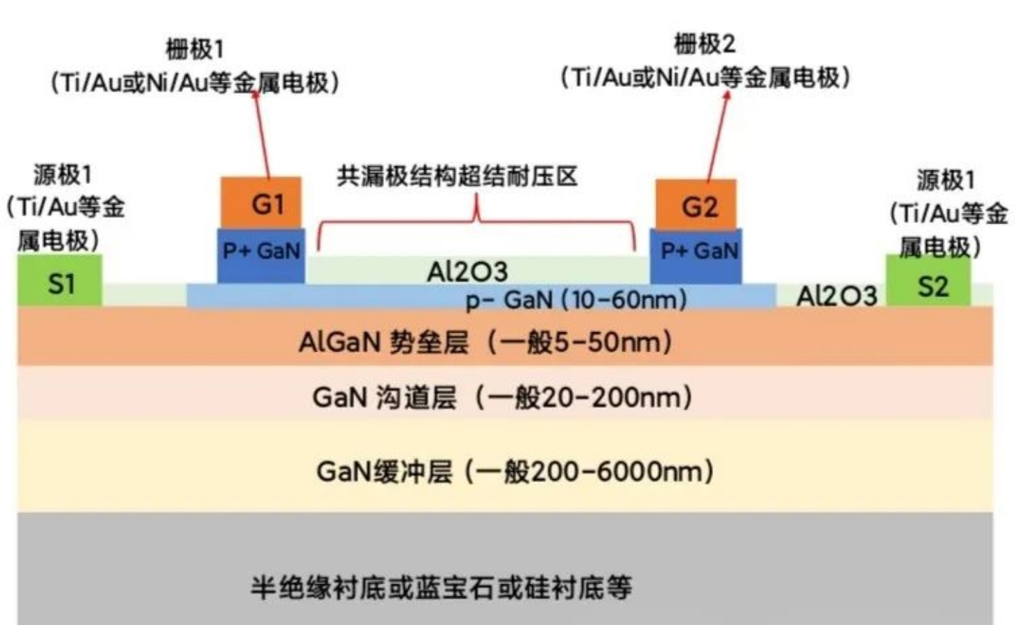
The Power P-GaN SJ BDS Gallium Nitride Superjunction Voltage Resistant Bidirectional Switching Device places all the surge electrical stresses of the original transverse PSJ and transverse p-GaN ReSURF more concentrated on the line closest to the edge of the polarization structure,
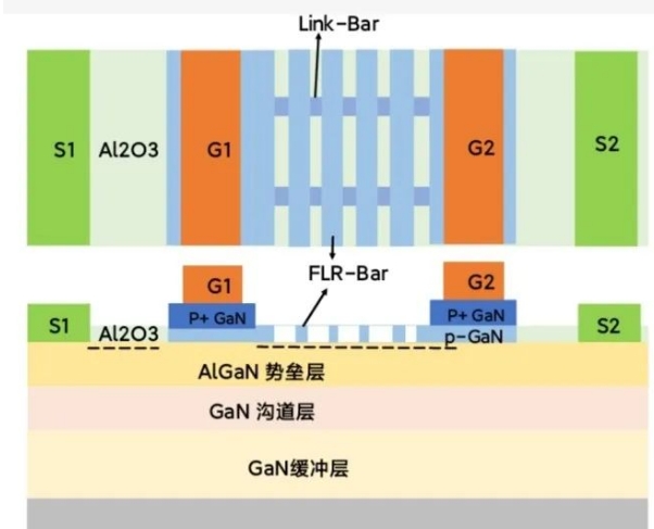
There are reliability issues with overload surges, and the large capacitance of the ReSURF field board exacerbates the problem of hot electron injection from overload surges in this area. So Erbao thought about it and decided not to create multiple field limiting rings similar to p-GaN thin layers, all connected to the drain to form a uniform voltage divider, while simultaneously considering the RESURF super junction voltage resistance structure.
So, try making another bidirectional voltage resistant switch?
What name should I choose? Power P-GaN SJ BDS Gallium Nitride Superjunction Voltage Resistant Bidirectional Switching Device?
A friend left a message asking me, didn't you share and discuss the structure of new gallium oxide devices at the Nanjing meeting on Saturday, Erbao? Can this super junction bidirectional switching device SJ BDS structure be used for gallium oxide devices?
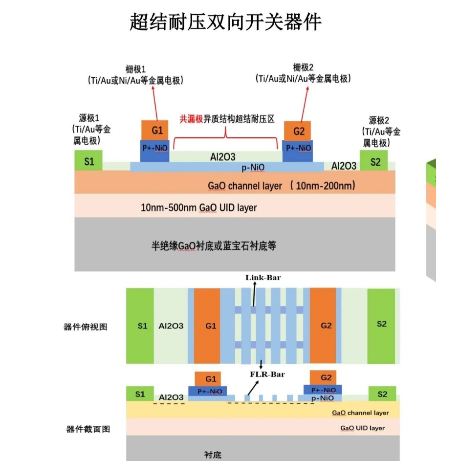
Of course, Erbao also wants to give it a try. If one day In the second round, Nakamura Shuji discovered a new buffer growth technology that can directly grow single crystal quasi single crystal quality gallium oxide epitaxial layers on different substrates such as silicon wafers/sapphire wafers. Perhaps in the future, gallium oxide materials will shine brightly in the field of heterogeneous epitaxial lateral high-voltage devices, and even high-voltage integrated ICs, and even replace GaN or silicon carbide devices in many fields?
The heterojunction bidirectional switching device composed of gallium oxide (Ga ₂ O3) and p-type nickel oxide (p-NiO) is a new type of power electronic device. Its working principle combines the characteristics of wide bandgap semiconductor materials, heterojunction band engineering, and superlattice structure design to achieve high voltage resistance, low loss, and bidirectional controllable switching function. The following is a detailed analysis of its working principle:
---
**1. Material and structural characteristics**
-Gallium oxide (Ga ₂ O3):
-Ultra wide bandgap semiconductor (bandgap width of about 4.8-4.9 eV), with extremely high critical breakdown electric field (about 8 MV/cm), suitable for high-voltage applications.
-Natural n-type conductivity, but lacking stable p-type doping, requires the introduction of p-type materials (such as p-NiO) through heterojunctions.
-* * p-type nickel oxide (p-NiO) * *:
-A p-type transparent conductive oxide forms a heterojunction with Ga ₂ O3 to compensate for the p-type defects of Ga ₂ O3 and provide hole injection capability.
-The alignment of heterojunction interface bands is crucial for carrier transport (which may form Type II band structures and promote charge separation).
-Superjunction structure:
-Composed of alternating p-NiO and n-Ga ₂ O3 regions, the transverse electric field distribution is optimized through charge balance, significantly improving the breakdown voltage while reducing the on resistance.
---
*2. Bidirectional switch mechanism**
**(1) Blocked state (off state)**
-* * Forward and reverse blockade * *:
-Under bidirectional voltage, the heterojunction interface and superlattice structure expand uniformly distributed electric fields through depletion regions, avoiding local electric field concentration.
-The charge balance of a super junction allows the longitudinal electric field (perpendicular to the junction direction) to be shared by the transverse electric field (parallel to the junction direction), significantly increasing the breakdown voltage (up to several thousand volts).
**(2) Conductive state (open state)**
-Bidirectional carrier injection:
-Forward bias voltage (Ga ₂ O3 terminal connected to positive):
The holes of p-NiO are injected into Ga ₂ O ∝, and the electrons of Ga ₂ O ∝ are injected into p-NiO, reducing the heterojunction potential barrier and forming bipolar conduction.
-Reverse bias voltage (Ga ₂ O3 terminal connected to negative):
Through the symmetrical design of the superlattice structure, a conduction path is also formed at the interface between p-NiO and Ga ₂ O3 under reverse bias, achieving bidirectional current flow.
-The high doping concentration of the superlattice structure further reduces the on resistance (Ron) and improves efficiency.
**(3) Switch triggering mechanism**
-Voltage triggered:
-When the applied voltage exceeds the threshold, avalanche breakdown or tunneling effect occurs in the depletion region of the heterojunction, causing carrier multiplication and rapid conduction of the device.
-Field control effect:
-Active switching control is achieved by regulating the heterojunction barrier height through gate (if designed) or structural electric field.
---
**3. Key advantages**
-* * High voltage resistance * *: The super junction structure and the high breakdown field strength of Ga ₂ O3 work together to support blocking voltages in the thousands of volts range.
-Low conduction loss: The bipolar conduction mechanism (where electrons and holes participate in conduction together) reduces Ron and improves energy efficiency.
-Bidirectional Symmetry: The structural design ensures consistent electrical characteristics in both forward and reverse directions, making it suitable for AC circuits or bidirectional power control.
-High temperature stability: The wide bandgap material is resistant to high temperatures and suitable for harsh environmental applications.
---
**4. Potential applications**
-High voltage DC/AC converters, such as smart grids and electric vehicle charging systems.
-Solid state circuit breaker: Fast response, high reliability circuit protection.
-RF power devices: High frequency, high-power communication systems.
---
**5. Challenges and research directions**
-Interface optimization: The interface defects of Ga ₂ O ∝/p-NiO heterojunctions may affect carrier transport and need to be improved through annealing or interface passivation.
-* * Thermal management * *: Ga ₂ O ∝ has low thermal conductivity and needs to be combined with heat dissipation design (such as diamond substrate integration).
-* * Process compatibility * *: Heteroepitaxial growth and superlattice manufacturing have high process complexity and require the development of low-cost mass production technologies.
---
**Summary**
Gallium oxide/p-NiO heterojunction bidirectional switching devices achieve high-voltage bidirectional conduction and fast switching characteristics through the synergistic effect of heterojunction band engineering and superlattice charge balance design, which is expected to break through the performance limit of traditional silicon-based devices and promote the development of the next generation of high-power electronic systems.