Introduction
In 2025, within only half a year, leading MCU manufacturers such as ST, NXP, and Renesas almost simultaneously released automotive MCU products equipped with new embedded storage (such as PCM and MRAM), breaking the long-standing technical pattern of MCU dominated by embedded Flash. Although it is still too early to talk about "standard configuration", it is certain that new storage has leapt from "attempt" to "strategic layout" and has begun to have a profound impact on the MCU ecosystem.
In the past, MCU was a "small and beautiful" device used for basic control logic. But in recent years, it is evolving towards "small and strong": the process has moved from traditional 40nm to 22nm, 16nm and even more advanced nodes; integrated AI acceleration, security unit, wireless module... Become a candidate for the "car brain" and "edge computing center".
Behind this, a long-ignored but crucial technology is "making up for the shortcomings": the revolution of embedded storage technology (eNVM).
Under the trend of "software-defined cars", OEMs and Tier1 manufacturers face unprecedented challenges: ECU complexity surges, functions are highly concentrated; OTA updates, AI reasoning, model loading, software "gets thicker and thicker"; storage space and read-write performance have become bottlenecks in the entire vehicle architecture. Traditional Flash has long been unable to keep up with the density, speed, power consumption and durability. In this context, new memories (PCM, MRAM) have become the key weapon for the evolution of MCUs.
ST chooses phase change memory (PCM)
Phase change memory (PCM) is an emerging non-volatile storage technology. Its basic principle is to store information through the phase change of materials (from amorphous to crystalline). The basic mechanism of PCM was invented by Robert Ovshinsky of Stanford University in the 1960s. STMicroelectronics has a patent license for this original development, and ST is the first manufacturer to truly implement PCM in automotive-grade MCUs.
ST also introduced the working principle of PCM on its official website. PCM is made of germanium antimony tellurium (GST) alloy. During the manufacturing process, it uses the physical property of the material that can undergo rapid thermal control changes between amorphous and crystalline states. The above states correspond to logic 0 and logic 1, respectively, and can be electrically distinguished by the high resistance of the amorphous state (logic 0) and the low resistance of the crystalline state (logic 1). PCM supports read and write operations at low voltages and has several substantial advantages over Flash and other embedded memory technologies.
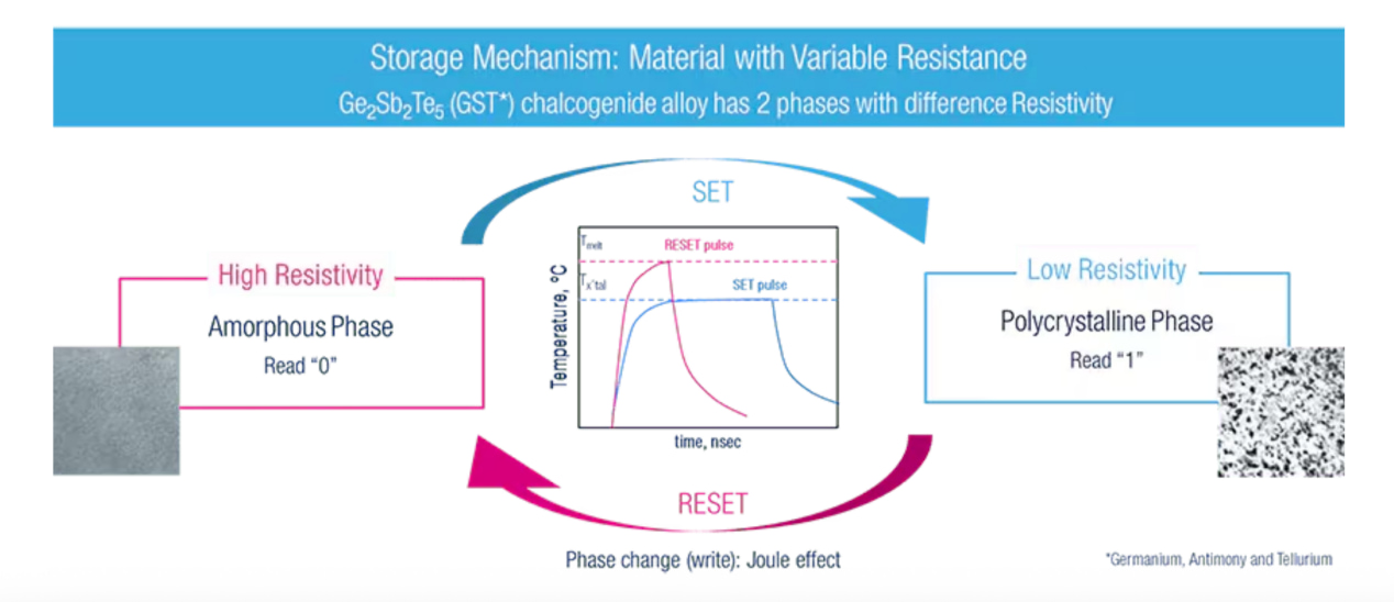
Working principle of PCM (Source: ST)
After years of research and development, in April 2025, ST launched Stellar with xMemory, a new generation of scalable memory embedded in its Stellar series of automotive microcontrollers. The core of Stellar xMemory is STMicroelectronics' proprietary phase change memory (PCM) technology. STMicroelectronics claims that it has the industry's smallest qualified storage bit unit, which can completely change the challenging process of developing software-defined vehicles (SDVs) and evolving electrification platforms.
It is reported that ST's Stellar P and G series automotive MCUs will be equipped with the latest generation of PCM technology using xMemory. The Stellar P and Stellar G series are Stellar Integration MCUs suitable for centralized regional controllers, domain controllers and body applications. The first to be launched will be the Stellar P6 MCU, which is designed to meet the needs of new powertrain trends and architectures for electric vehicles (EVs) and will be put into production in the second half of 2025.
Stellar with xMemory technology does not need to manage multiple devices with different memory options, nor does it need to bear the related development and certification costs. It only needs one innovative device with scalable memory to provide customers with efficient and economical solutions. This simplified approach from the beginning enables automakers to design for the future and leave more room for innovation later in the development cycle, thereby reducing development costs and accelerating time to market through a more streamlined supply chain.
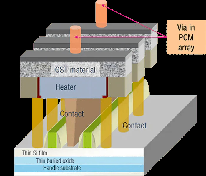
Cross-section of an embedded PCM bit cell in FD-SOI technology, showing the heating device that quickly flips the memory cell between crystalline and amorphous states.
ST points out that choosing the right MCU early in the SDV life cycle ensures that there is sufficient on-chip memory for future software development. Today, choosing too high a memory specification increases costs, while choosing too low a memory specification may require the subsequent search and re-qualification of other MCUs with additional memory, adding complexity, cost and delay. Stellar MCUs with xMemory are highly competitively priced, providing more cost savings, simplifying the OEM supply chain, and shortening certification time by extending product lifecycles and maximizing reuse between projects, thereby accelerating time to market.
NXP and Renesas, Embracing MRAM
Magnetoresistive RAM (MRAM) is another type of non-volatile storage "black technology". MRAM uses the physical properties of magnetic materials to achieve data storage, with ultra-high write speeds, low power consumption and extremely strong durability. MRAM has been widely adopted by companies such as NXP and Renesas.
NXP is an early automotive MCU manufacturer to launch MRAM MCU. In March this year, NXP Semiconductors announced the launch of its S32K5 series of automotive MCUs, the industry's first MCU based on 16nm FinFET process with built-in MRAM, marking an important milestone in its development. The S32K5 series is designed to expand the NXP CoreRide platform, providing pre-integrated regional and electrification system solutions to support the evolution of scalable software-defined vehicle (SDV) architectures.
Automakers are increasingly adopting partitioned architectures, each with its own unique approach to integrating and distributing the functions of electronic control units (ECUs). At the heart of these solutions is an advanced MCU architecture that combines real-time performance with low latency, deterministic communications and innovative isolation capabilities.
The addition of high-performance MRAM significantly speeds up ECU programming, both at factory settings and during over-the-air (OTA) updates. MRAM writes more than 15 times faster than traditional embedded flash memory, enhancing the flexibility of automakers to deploy new software features throughout the life cycle of the vehicle.
In July 2025, Renesas also released an MCU with built-in MRAM, but compared with NXP, the process is 22nm. The device is equipped with 1MB MRAM and 2MB SRAM. It is said that the use of MRAM is a major feature of the second-generation RA8 series. In addition to high durability and data retention, MRAM also has advantages such as high-speed reading and writing, no need to erase, and low power consumption. Renesas Electronics released MRAM high-speed reading and writing technology for high-performance microcontrollers at the International Semiconductor Integrated Circuit Conference (ISSCC 2024), and RA8P1 uses this technology.
For applications that require larger memory capacity, the device is equipped with an eight-way SPI interface and a 32-bit external bus interface that supports XIP/DOTF. In addition, system-level package (SiP) products with integrated 4MB or 8MB external flash memory are also available. In terms of peripheral functions, it supports parallel camera input, MIPI-CSI2, serial audio input, and multimodal AI voice input through PDM. In addition, it is also equipped with a 16-bit AD converter, graphic HMI function, and various serial interfaces.
TSMC: MRAM and RRAM go hand in hand
As the world's leading foundry, TSMC has bet on two major technologies for new storage technologies: MRAM and RRAM.
At the 2025 Technology Seminar, Dr. Yujie Mi, Executive Vice President and Co-Chief Operating Officer of TSMC, pointed out: "eFlash technology has encountered expansion bottlenecks at the 28nm process node, and the new generation of NVM (non-volatile memory) must replace its role in more advanced processes."
As a result, TSMC clearly proposed to introduce two embedded storage technologies, RRAM and MRAM, into 22nm, 16nm, and 12nm, respectively, and further advance to 6nm and 5nm nodes.
TSMC is one of the few manufacturers that has achieved large-scale mass production of RRAM. At present, TSMC has achieved mass production of RRAM on 40nm, 28nm and 22nm processes, and has passed automotive-grade certification. 12nm RRAM has also entered the customer tape-out stage, and the 6nm version is underway. Infineon's new generation of AURIX MCU uses TSMC's eRRAM technology, which has become an important embedded storage solution for its automotive platform.
The advantages of RRAM are: low process complexity, can be directly deployed in the back-end metal layer (BEOL); fully compatible with logic process, adaptable to multiple types of MCU architectures; especially suitable for power-sensitive and cost-intensive consumer and automotive applications.
In contrast, although MRAM has a more complex process, it has superior performance characteristics: the write speed is more than ten times that of Flash; non-volatile storage + extremely strong durability; suitable for scenarios that require high-speed writing, frequent OTA updates, AI reasoning and other complex tasks. For in-vehicle computing platforms (such as ADAS, AI SoC, etc.) that pursue computing power density, data throughput and real-time performance, MRAM may be the most ideal storage replacement after eFlash.
TSMC has currently achieved mass production of MRAM at the 22nm process node, 16nm MRAM has entered the customer preparation stage, and 12nm is under development. A more radical roadmap also includes future expansion to 5nm nodes.
In May 2025, TSMC announced that it would set up its first European Design Center (EUDC) in Munich, Germany, focusing on R&D and customer support for MRAM storage technology for automotive applications. This center will become TSMC's tenth design center in the world and is scheduled to be officially opened in the third quarter of 2025. Its service areas include automotive, industrial, AI, telecommunications and the Internet of Things. This also means that TSMC not only promotes the popularization of new storage on the process platform, but also deepens the vehicle development ecosystem in its global layout.
In addition to horizontally advancing process nodes, TSMC is also seeking technological breakthroughs in the following directions:
3D RRAM MCU: Promote embedded storage stacking packaging to free up more on-chip space; SOT MRAM (spin-orbit torque): Compared with traditional STT-MRAM, it has lower power consumption and faster writing speed, and is expected to enter large-scale mass production; Silicon photonics platform: Combine optical interconnection and storage interface, and layout for data centers and edge computing.
The implementation of these technologies will further consolidate TSMC's leading position in specialty processes and embedded storage ecosystems.
Storage and computing integration trend
Whether it is PCM, MRAM or RRAM, they are not only memory substitutes, but also catalysts for MCU architecture changes. New storage technologies such as PCM, MRAM and RRAM represent a deeper trend of "storage and computing integration", which is not just a simple storage medium replacement issue, but a coordinated evolution between storage architecture and computing architecture.
In the field of MCU, the boundaries between storage and computing are becoming increasingly blurred. In traditional MCUs, storage and computing are separate modules. Computation is performed through the central processing unit (CPU) or dedicated accelerators, while storage is performed through external or internal flash memory, SRAM and other devices for data storage and management. However, with the complexity of computing tasks, especially the growing application demand for machine learning, AI reasoning and edge computing, the separation of storage and computing is becoming increasingly unsuitable.
The addition of new memories such as MRAM and PCM provides a new opportunity for "storage and computing integration". In particular, PCM, through its phase change characteristics, not only has non-volatile storage functions, but also can play the role of "near computing" in some applications, reducing the bottleneck of data transmission and further accelerating the data processing process. MRAM's high-speed read and write characteristics also enable it to work with computing modules to improve processing efficiency in scenarios such as AI edge reasoning and real-time data processing.
In today's AI edge, OTA fragmentation, and software agility, the "intelligence" of MCUs is increasingly dependent on memory capabilities. It is expected that future MCU architectures will increasingly combine storage and computing to create more efficient, flexible, and intelligent systems.
Conclusion
In the past decade, we have been accustomed to viewing MCUs as representatives of "control" systems, and their embedded storage is just a supporting component; but in the era of AI, SDV, and edge intelligence, storage is moving from behind the scenes to the front, becoming an integral core of computing architecture. This is not only a replacement of materials and an evolution of processes, but also a key step for MCUs to move from "usable" to "scalable" and "evolvable".
In this wave of microcontroller upgrades triggered by embedded storage, we see not only the differentiation of the routes of leading manufacturers, but also the accelerated adaptation and evolution of the entire industrial chain - from foundry to tool chain, from automobiles to industrial applications. This transformation has just begun.